
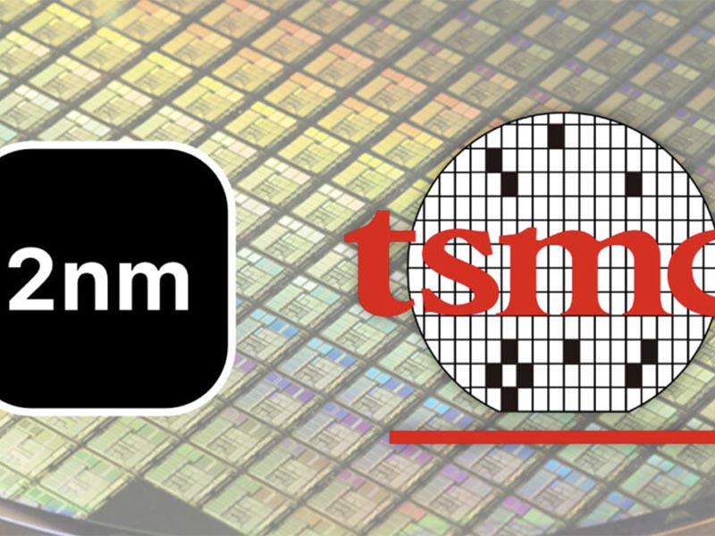
Why TSMC’s 2nm Process Node Is Set to Reshape the Semiconductor Industry
Discover how TSMC’s 2nm process, powered by GAA nanosheet transistors, is revolutionizing semiconductor manufacturing. Learn about its advantages, key differences from competitors, and implications for AI, mobile, and industrial applications.
🧠 Introduction
As global demand for AI, high-performance computing (HPC), and energy-efficient mobile devices continues to surge, the semiconductor industry is locked in a race toward smaller, faster, and more efficient chips.
At the forefront of this race is Taiwan Semiconductor Manufacturing Company (TSMC) — the world’s leading foundry.
With its 2nm (nanometer) process node, TSMC is redefining the limits of silicon technology, setting new benchmarks for performance, power efficiency, and scalability.
This article explores what makes the 2nm node revolutionary, how it compares with Intel and Samsung, and what it means for the next generation of computing.
🔍 What Is a 2nm Process Node?
The term “2nm” refers to the process node — the smallest features that can be fabricated on a chip.
While no longer a direct measurement of physical gate length, it represents generational improvements in:
- Transistor density
- Switching speed
- Energy efficiency
Transitioning from 3nm to 2nm offers roughly 15–30% performance gain or 30–50% power reduction, depending on design optimization.
🧬 The Key Innovation: Gate-All-Around (GAA) Nanosheet Transistors
TSMC’s 2nm process introduces Gate-All-Around (GAA) transistors, replacing the long-dominant FinFET structure.
Unlike FinFETs — where the gate wraps around three sides of the channel — GAA completely surrounds it, improving electrostatic control and reducing leakage.
This architecture allows:
- Better performance scaling
- Lower power consumption
- Higher drive current in smaller footprints
It’s a crucial innovation for AI accelerators, smartphones, and energy-sensitive embedded devices.
⚙️ How TSMC’s 2nm Compares to Competitors
| Company | Process Node | Transistor Type | Mass Production | Key Markets |
|---|---|---|---|---|
| TSMC | 2nm (N2) | GAA Nanosheet | 2025 | AI chips, smartphones, HPC |
| Samsung | 2nm | GAA MBCFET™ | 2025 (early) | Mobile, automotive |
| Intel | 18A (~1.8nm) | RibbonFET (GAA) | Late 2024–2025 | Server & desktop CPUs |
While Samsung was first to announce a GAA roadmap, TSMC’s process maturity, yield, and supply chain scale make it the preferred choice for major clients such as Apple, AMD, NVIDIA, and Qualcomm.
⚡ Power Efficiency and Performance Gains
- 15% speed improvement at the same power
- Up to 30% power savings at the same speed
- ~20% increase in transistor density
These gains enable longer battery life in mobile devices, lower data-center power costs, and better thermal performance for edge AI systems.
🏠 Manufacturing Ecosystem and Fab Expansion
TSMC is investing heavily in global 2nm capacity:
- Fab 20 in Hsinchu, Taiwan
- Arizona Fab expansion in the United States
- Integration with 3DFabric technologies such as CoWoS and InFO for advanced packaging
These investments ensure supply stability and ecosystem readiness for global customers.
📱 Real-World Applications
- Smartphones: Next-generation iPhones and Android flagships
- Edge AI: Robotics, smart cameras, and autonomous systems
- Data Centers: AI training & inference accelerators
- Wearables: Ultra-efficient SoCs for compact devices
The 2nm process enhances both performance and efficiency across consumer and industrial markets.
🔐 Technical Challenges and Industry Solutions
While 2nm offers remarkable benefits, it also presents new challenges:
- Complex GAA design rules and EDA requirements
- Higher production costs per mask and wafer
- Tighter process control for nanosheet uniformity
TSMC mitigates these with advanced simulation tools and close partnerships with Cadence, Synopsys, and Arm, ensuring a robust design ecosystem.
🤝 What Comes After 2nm?
TSMC is already developing 1.4nm and beyond, with technologies such as:
- Backside Power Delivery Network (BPDN)
- 2D semiconductors (e.g., MoS₂, graphene)
- Chiplet-based modular architectures
These innovations will further push the boundaries of performance and integration for both high-end and embedded markets.
✅ Conclusion
TSMC’s 2nm process node represents a monumental step forward in chip manufacturing — driving the next generation of AI computing, mobile performance, and embedded intelligence.
For engineers and system designers, it’s not just about smaller transistors — it’s about enabling smarter, more energy-efficient systems that define the future of technology.